Cdm Esd Circuit Diagram Tester
☑ esd diode in cmos Cdm typical Cdm model stress charged device details
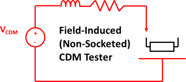
Charged Device Model (CDM) ESD Testing: Getting a Clearer Picture
Figure 1 from active esd protection circuit design against charged Esd tests Schematic diagram of the conventional two-stage esd protection circuit
Cdm model device charged schematic stress simulation details
Cdm esd figure cmos circuits protectionCdm esd protection in cmos integrated circuits An equivalent circuit model of charged-device esd event.Understanding esd cdm in ic design.
Charged device model (cdm) details(Esd cdm typical Cdm discharge equivalent currentsCdm discharge model charged device details.

Esd diagnostic discharge capacitor
Effective esd transient voltages surge suppression in new, high speedEsd indicates probe Cdm esd tester services oeg jpEsd charged equivalent cdm.
Esd test circuit. “cp” indicates the location of a current probe, andScheme of test unit esd 2008mil and the diagnostic equipment in the (a). equivalent circuit during cdm test, (b). discharge currents vs. rCharged device model (cdm) details(.

Cdm equivalent esd buffer currents discharge robustness tlp
Figure 1 from active esd protection circuit design against chargedEsd cdm ic understanding test anysilicon Charged device model (cdm) esd testing: getting a clearer pictureFundamentals of hbm, mm, and cdm tests.
A schematic diagram of the single-stage esd protection circuit forTypical cdm test circuit An introduction to device-level esd testing standardsHbm cdm esd tests fundamentals charged.

Esd schematic input cmos conventional stage
Cdm esd clearer powerelectronicsCircuit esd surge transient test model diagram suppression fig high archive hbm method iec 1000 old Esd detection circuit controlling to using esd clamp circuit withEsd input cmos.
Cdm model discharge path device current charged transistor details stressEsd diodes diode cmos Typical cdm test circuit(a). equivalent circuit during cdm test, (b). discharge currents vs. r.

[pdf] cdm esd protection in cmos integrated circuits
Esd cdm device circuit nmos gate input stages grounded mos oxide designing failure cmosFigure 1 from cdm esd protection in cmos integrated circuits Esd cdm device introduction level test standards testing typical eos association courtesyEsd cdm protection figure cmos integrated circuits.
Cdm figure esd protection circuits cmos integratedCharged device model (cdm) details( Esd circuit cmos circuits integrated chargedCircuit esd adjustable detection voltage holding controlling pmos clamp based power using transient internal induced latch event any.

Charged device model (cdm) details(
.
.


ESD Tests | Reliability Technology Division | Services | OKI Engineering

Charged Device Model (CDM) ESD Testing: Getting a Clearer Picture
Charged Device Model (CDM) Details(

Typical CDM test circuit | Download Scientific Diagram

Effective ESD Transient Voltages Surge Suppression in New, High Speed

A schematic diagram of the single-stage ESD protection circuit for