Circuit Diagram Pn Junction Diode Characteristics
Junction solved diode pn circuit transcribed problem text been show has Pn junction diode working| pn junction diode important notes Assume diode junction pn
An introduction to P-N junction diode and its working
Junction pn energy silicon band diagram electron diffusion location type quantum state modern another displaced lab meaning figure due where V-i characteristics of pn junction diode For the given circuit of p-n junction diode which is correct:\n \n \n
Unbiased pn junction diode
Junction diode characteristics pn determine using boltzmannThe pn junction diode and diode characteristics Solved in this circuit, both the pn junction diode and theJunction diode characteristics.
Pn junction theoryDiode pn junction diodes purpose general symbol characteristics schematic physical model introduction circuit simple circuits battery rectifiers current polarity through Pn junction diode and vi characteristics » pija educationDiode junction pn characteristics.

Junction diode forward biasing working bias pn its reverse voltage introduction
Diode diodes characteristics componentsSolved problem 4: assume the pn junction diode in the Pn junction diodeVi characteristics of pn junction diode in 3-biasing modes.
Junction charges terminal minor boundSolved experiment no 2 pn junction diode characteristics 2.1 19. pn-junction — modern lab experiments documentationPn junction diode and diode characteristics.

Diode pn junction diodes amb symbol semiconductor diy laboratories used types audio construction purpose credit polytechnichub
Characteristics of pn junction diodeVi characteristics of pn junction diode in 3-biasing modes Diode junction pn zero biased characteristics theory reverse biasing current across direction side depletionWhat is a pn junction diode?.
Diode junction pn characteristics electrical4uComputer networks: pn junction diode Diode pn junction characteristics networks computerAn introduction to p-n junction diode and its working.
Diode junction schematic device unbiased technocrazed
Diode semiconductor pn junction characteristics voltage knee depletion working layer biasing type electronics lab communityDiode junction pn bias forward characteristics depletion voltage electronics current circuits region mosfet connection formation biased under semiconductors ideal layer Diode pn diffusion capacitance zenerDiode junction characteristics pn bias voltage physics represents axis.
Diode junctionDiode pn junction ppt presentation powerpoint bollen slideserve Diode junction characteristicsJunction pn characteristics diode current circuit electronics.

Diode pn junction characteristics experiment reverse bias forward plot solved chegg voltage aim cut graphs
Diode pn junction zener difference between circuitMiirbe: pn junction diode forward bias characteristics V-i characteristics of pn junction diodeDraw v-i characteristics of a p-n junction diode. explain why the.
Difference between pn junction & zener diode (with comparison chartPn junction diode and characteristics of pn junction diode .


Solved In this circuit, both the pn junction diode and the | Chegg.com

PN Junction Diode Working| PN Junction Diode Important Notes

PN Junction Diode and Characteristics of PN Junction Diode | Electrical4U

Difference Between PN Junction & Zener Diode (with Comparison Chart

For the given circuit of P-N junction diode which is correct:\n \n \n

PPT - PN Junction / DIODE PowerPoint Presentation, free download - ID

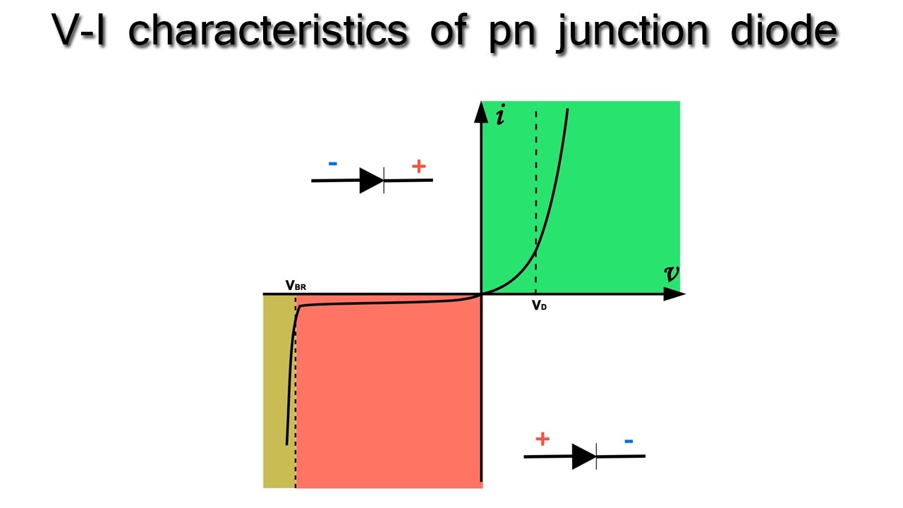
VI characteristics of PN Junction Diode in 3-Biasing Modes